Applications
R&D for Bonding Materials
Episode03
Our technology is flexible enough to cope with even the challenging semiconductor thinning process.
We propose solutions that are essential to next-generation technologies and are also involved in efforts to develop bonding materials with novel functions.
0103
Contributing to the Wafer and Support Bonding Process
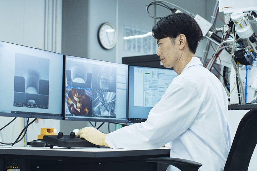
With the miniaturization of semiconductors, semiconductor wafers are becoming increasingly thinner. In order to create the thinnest wafers (approximately 40 microns), a bonding process to bond a wafer to a support such as glass is required. While various industrial resins have been developed for manufacturing purposes, not many are able to withstand the semiconductor thinning process. The polyimide resin that we developed is.

0203
Enabling Detachment from a Support with a Laser n
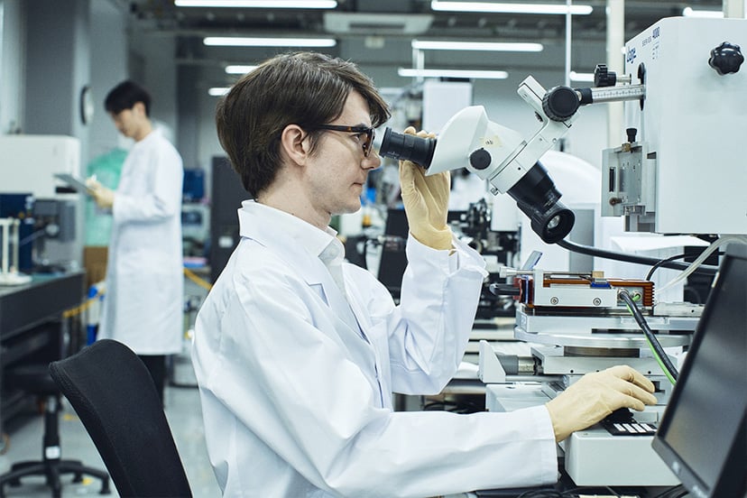
When used for bonding, our polyimide products are also superior in terms of heat resistance and chemical resistance. Polyimide-based semiconductor bonding technology ensures strong resistance to heat treatment, mechanical stress, and chemicals to enable the sophisticated processing sought by customers.
Moreover, following processing performed using our technology, it is possible to detach a wafer from the support using a laser with minimal mechanical damage to devices.
0303
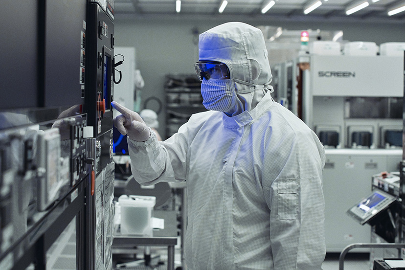
Offering Solutions Essential to Next-generation Technologies
Using polyimide-based bonding technology allows the selective picking and placing of the desired semiconductor chips by backside treatment or partial laser radiation following temporary polyimide bonding. This technology is indispensable for the success of the micro-LED display technology, a vivid, next-generation liquid crystal display technology following on from organic EL. Having been developing products needed for stacking IC devices, we can offer various solutions according to each customer’s needs.